Intel Announces 288-Core Sierra Forest CPU, 5th-Gen Xeon Arrives December 14

288-core CPU
(Image credit: Tom's Hardware)

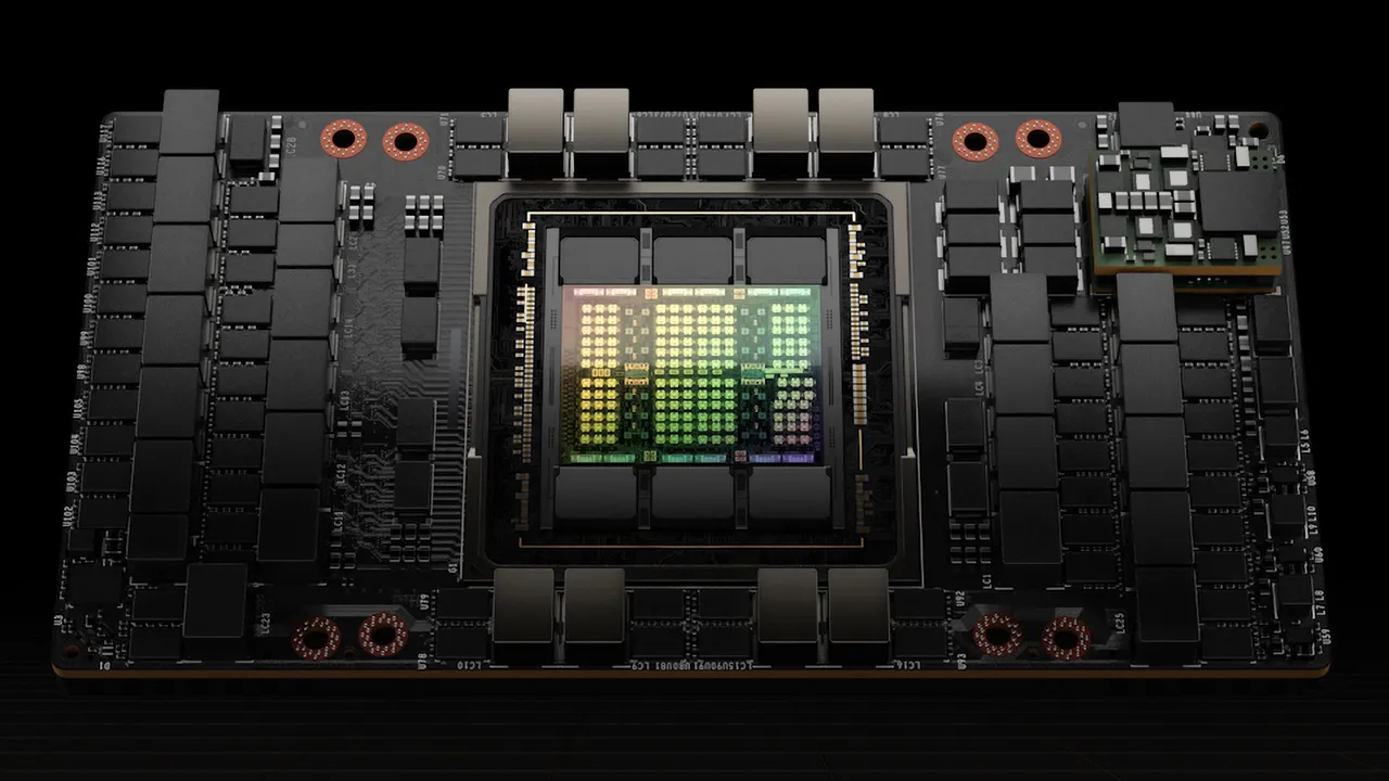
Intel CEO Pat Gelsinger announced at the company’s Innovation 2023 conference that it has a new Sierra Forest Xeon processor with 288 E-cores coming to market in the future. Each core is single-threaded, so Intel’s new chip packs 288 physical cores and comes on the heels of Intel’s previously announced 144-core Sierra Forest processors. Intel also announced that its fifth-gen ‘Emerald Rapids’ Xeon will arrive on schedule on December 14. 

The new Sierra Forest chips wield an E-core-based architecture that delivers the ultimate in threaded heft for scale-out, cloud-native, and containerized environments. You can read the deep dive architectural details here, but the big takeaway is that the chips employ CPU chiplets with the Intel 3 process combined with twin I/O chiplets based on the Intel 7 node to provide a flexible architecture that can scale to higher core counts with the addition of more chiplets.  

The new 288-core model isn’t entirely surprising, as the company’s Granite Rapids architecture, which it also uses for Sierra Forest, can accommodate up to three compute chiplets packed with cores. Intel can pack 144 E-cores into a single chiplet. 

Intel recently slipped and accidentally revealed what is thought to be its 144-core Sierra Forest chip package in a press video that was later redacted. The large center die houses the CPU cores, while the two smaller die house I/O functions. We calculated that this single 588mm^2 I/O die can accommodate the originally-announced 144 E-cores in the center die, but Intel has Granite Rapids chips based on this same design that come with up to three compute chiplets.  

As you can see in the above album, Granite Rapids and Sierra Forest share the same overall design, but the former comes with variants that can house one, two, or three CPU chiplets. Intel’s new 288-core behemoth simply employs two of the E-core-laden dies to reach its higher core counts. That means Intel could also release a model with three CPU chiplets, thus totaling 432 cores in a single massive chip. Of course, memory bandwidth, thermals, and TDP could be factors that prevent a three-chiplet monster, but only time will tell.

Swipe to scroll horizontally
Row 0 - Cell 0 202320242025
Intel P-CoresEmerald Rapids - Intel 7 | Sapphire Rapids HBMGranite Rapids - Intel 3Row 1 - Cell 3
AMD P-Cores5nm Genoa-XTurin - Zen 5
Intel E-Cores1H - Sierra Forest - Intel 3 -144 CoresClearwater Forest - Intel 18A
AMD E-Cores1H - Bergamo - 5nm - 128 Cores

Here we can see how Intel’s roadmap looks next to AMD’s data center roadmap. AMD’s competing 128-core, 256-thread Bergamo takes a very similar core-heavy approach as Sierra Forest by leveraging AMD’s dense Zen 4c cores. Bergamo is already on the market, while Intel’s first Sierra Forrest chips won’t arrive until the first half of 2024. AMD hasn't outlined its second-gen Zen 4c model. Intel now has its second-gen E-core-powered Clearwater Forest on the roadmap for 2025. 

Intel also announced that its fifth-gen ‘Emerald Rapids’ Xeon arrives on-schedule on December 14, which is a good sign as the company’s roadmap remains on track. Emerald Rapids will face off with AMD’s 5th-gen EPYC Turin chips that launch before the end of 2024. 

Paul Alcorn
Deputy Managing Editor

Paul Alcorn is the Deputy Managing Editor for Tom's Hardware US. He writes news and reviews on CPUs, storage and enterprise hardware.

  • bit_user
    Edit: Correction noted. Thanks!
    ---
    Here's the remaining informational content of my post, in case anyone missed it:
    Emerald Rapids is built on Intel 7. Likely the same iteration of it that was used for Raptor Lake. Granite Rapids and Sierra Forest are using Intel 3. They're the first announced products to use it.
    @PaulAlcorn , as usual, thanks for your excellent coverage!
    : )
    Reply
  • Homeman
    "Moore's law is dead!" yee
    Reply
  • bit_user
    Homeman said:
    "Moore's law is dead!" yee
    On that front, it's more instructive to look at the announced roadmaps of IFS, TSMC, and Samsung. They tell you what improvements on density, power, and performance to expect. You needn't wait for actual product announcements to see what those nodes can do.
    https://www.anandtech.com/show/16823/intel-accelerated-offensive-process-roadmap-updates-to-10nm-7nm-4nm-3nm-20a-18a-packaging-foundry-emib-foveroshttps://www.anandtech.com/show/18832/tsmc-outlines-2nm-plans-n2p-brings-backside-power-delivery-in-2026-n2x-added-to-roadmaphttps://www.anandtech.com/show/18936/samsung-updates-foundry-roadmap-2nm-in-2025-14nm-in-2027
    The power & performance metrics are somewhat artificial, because they presume the exact same microarchitecture. So, treat them as a lower bound, in terms of performance and efficiency, and an upper bound on density.

    And, for a really long-range view (but without specific performance metrics), you should look to IMEC:
    https://www.tomshardware.com/news/imec-reveals-sub-1nm-transistor-roadmap-3d-stacked-cmos-20-plans
    Reply
  • Homeman
    bit_user said:
    On that front, it's more instructive to look at the announced roadmaps of IFS, TSMC, and Samsung. They tell you what improvements on density, power, and performance to expect. You needn't wait for actual product announcements to see what those nodes can do.
    https://www.anandtech.com/show/16823/intel-accelerated-offensive-process-roadmap-updates-to-10nm-7nm-4nm-3nm-20a-18a-packaging-foundry-emib-foveroshttps://www.anandtech.com/show/18832/tsmc-outlines-2nm-plans-n2p-brings-backside-power-delivery-in-2026-n2x-added-to-roadmaphttps://www.anandtech.com/show/18936/samsung-updates-foundry-roadmap-2nm-in-2025-14nm-in-2027
    The power & performance metrics are somewhat artificial, because they presume the exact same microarchitecture. So, treat them as a lower bound, in terms of performance and efficiency, and an upper bound on density.

    And, for a really long-range view (but without specific performance metrics), you should look to IMEC:
    https://www.tomshardware.com/news/imec-reveals-sub-1nm-transistor-roadmap-3d-stacked-cmos-20-plans

    I am picking up info - piece by piece. I am currently not looking up specific news about hardware. I just came across this announcement and thought "Oh well, people on the net used to say "moore's law is dead"" but then again it is just my own ignorance to talk before making comprehensive research. Anyway, I appreciate your time - have a good one
    Reply
  • bit_user
    Homeman said:
    I am picking up info - piece by piece. I am currently not looking up specific news about hardware. I just came across this announcement and thought "Oh well, people on the net used to say "moore's law is dead"" but then again it is just my own ignorance to talk before making comprehensive research. Anyway, I appreciate your time - have a good one
    What worries me is the cost of new nodes. What I think we're likely to see is more of a "fizzling out", rather than smacking hard into a wall, due to increasing cost of new nodes, while the returns diminish.

    They touched on this more, in a slightly earlier IMEC article:
    Source: https://www.tomshardware.com/news/imecs-sub-1nm-process-node-and-transistor-roadmap-until-2036-from-nanometers-to-the-angstrom-era
    Also, this (though, getting a bit dated):
    Source: https://www.quora.com/If-the-Moores-law-is-slowing-down-can-the-slow-down-be-solved-by-increasing-the-size-of-the-chip-so-the-chip-can-have-more-free-space-where-more-transistors-will-be-put-If-this-is-not-a-good-solution-what-other
    If anyone finds a plot with newer nodes, please share!


    Oh, and SRAM scaling has essentially stopped. Perhaps more exotic, multi-layer cell designs will achieve better areal density. But, to the above point, that won't come without additional cost.
    https://fuse.wikichip.org/news/7343/iedm-2022-did-we-just-witness-the-death-of-sram/
    Reply
  • bit_user
    bit_user said:
    If anyone finds a plot with newer nodes, please share!
    Found it!

    Source: https://www.semianalysis.com/p/a-century-of-moores-law
    Reply
  • gg83
    How do Intels high e-core chips compare to the high arm core count chips?
    Reply
  • cyrusfox
    bit_user said:
    What worries me is the cost of new nodes. What I think we're likely to see is more of a "fizzling out", rather than smacking hard into a wall, due to increasing cost of new nodes, while the returns diminish.
    And hence the rapid adoption of advance packaging with full chip disaggregation. enabling utilization of advance node only where it shows ROI benefit.
    Reply
  • bit_user
    gg83 said:
    How do Intels high e-core chips compare to the high arm core count chips?
    We don't know, yet. Sierra Forest isn't due out until mid-2024 and will use the Crestmont mircroarchitecture on Intel 3. So, there are way too many variables to form a reasonable extrapolation from the data we have on the current low core-count Gracemont CPUs using Intel 7.

    I should add that Xeons tend to sample a lot sooner than consumer CPUs - possibly up to a year, in advance. So, I wouldn't be surprised if there are already (or soon to be) some engineering samples floating around, with the inevitable benchmark leaks soon to follow.
    Reply
  • bit_user
    cyrusfox said:
    And hence the rapid adoption of advance packaging with full chip disaggregation. enabling utilization of advance node only where it shows ROI benefit.
    Yeah, but if you just look at that delidded 288-core CPU, the majority of the die area is still very much in the compute dies, which are made on the most advanced node. No doubt the chiplets & mixed-node thing helps, but it's not a panacea.

    Yes, chiplets still help with improving yield, but each die-hop is energy-intensive, so you don't want to get carried away. That's probably why their compute dies are each 578 mm^2, which is non-trivial even on current, mature nodes.
    Reply