▶ Intel Details Core Ultra ‘Meteor Lake’ Architecture, Launches December 14
▶ Intel's Meteor Lake GPU Doubles Integrated Graphics Performance Per Watt
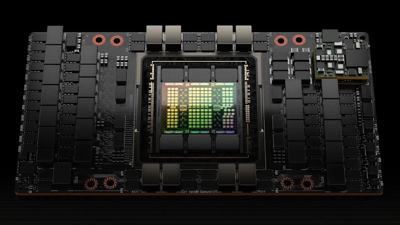
▶ Intel Announces 288-Core Processor, 5th-Gen Xeon Arrives December 14
▶ Intel Displays Arrow Lake Wafer With 20A Process Node, Chips Arrive in 2024
▶ Intel Flashes World’s First UCIe-Connected Chiplet-Based CPU
▶ Intel Shows Off Lunar Lake-Based PC, Unveils Panther Lake for 2025
Intel CEO Pat Gelsinger displayed a wafer filled with Arrow Lake test dies based on the 20A process node here at Intel Innovation 2023, saying the chips remain on-track for launch in 2024. If Intel stays on track with its 20A node, it will beat TSMC to two critical new chipmaking technologies. Gelsinger also said that Intel’s plan of delivering five nodes in four years remains on track, with the Intel 4 node ready for manufacturing and the Intel 3 node on-schedule for the end of the year.

Intel’s next-gen Meteor Lake chips, the first to use the 'Intel 4' node, are in production and on schedule for launch later this year. These will be the company's first high-volume consumer chips to use a chiplet-based architecture tied together with the 3D Foveros interconnect tech.
Intel's next-next-gen Arrow Lake chips build on that same design methodology with a newer Intel 20A process node, which comes with plenty of new additions that could propel Intel into the lead over TSMC with new transistor technology.

Arrow Lake will be Intel’s first to use Intel's 20A node (2nm), which includes new innovations like the PowerVia backside power delivery. This technique routes all power for the transistors directly through the backside of the transistor, partitioning power delivery to the backside of the transistors while data transmission interconnects remain in their traditional location on the other side.
This produces a host of benefits that includes enabling denser transistor arrays, improving voltage droop characteristics to unlock higher frequencies, and allowing for faster transistor switching while enabling denser signal routing on the top of the chip. Signaling also benefits because the simplified routing enables faster wires with reduced resistance and capacitance.
Intel will lead the industry with the first mass-produced chips with backside power delivery in 2024. TSMC won’t integrate this technology until 2026.

Intel’s 20A process also includes RibbonFet Gate-All-Around (GAA) technology, which is Intel’s first new transistor design since FinFET arrived in 2011. Intel's design features four stacked nanosheets, each surrounded entirely by a gate. Intel claims this design enables faster transistor switching while using the same drive current as multiple fins, but in a smaller area. This certainly seems plausible; We've already seen several chipmakers embrace different variations of this transistor technology.
Intel says that its 18A node remains on track to be manufacturing-ready in the second half of 2024. TSMC plans for its N2 node with GAA to arrive in 2025, so it will be the last to adopt the new type of transistor. Samsung was the first to produce GAA for shipping products, but the low-volume SF3E pipe-cleaner node won't see mass production. Instead, the company says it will debut its advanced node for high volume manufacturing later this year.
Overall, Intel claims to be on-track to deliver on its goal of delivering five nodes (technically six) in four years. The finer details of Arrow Lake, like core counts and configurations, remain unknown.
We’re here at the show and will update with additional details about the new Arrow Lake processors as they emerge.