Unlike its rivals AMD and Intel, Nvidia yet has to implement a multi-chiplet design for high-performance compute GPUs, but it looks like the company might be on track to finally use this design layout with its next-generation Blackwell generation of GPUs. At least so says renowned hardware leaker @kopite7kimi, who tends to have accurate information about Nvidia's intentions. For now, this is all a pure speculation though.
"After the dramas of GA100 and GH100, it seems that GB100 is finally going to use MCM," @kopite7kimi wrote in an X post. "Maybe GB100=2*GB102."
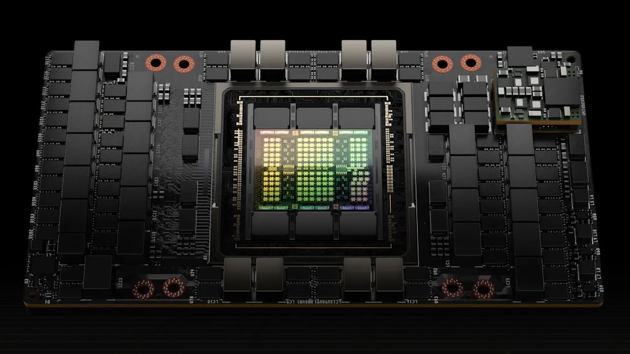
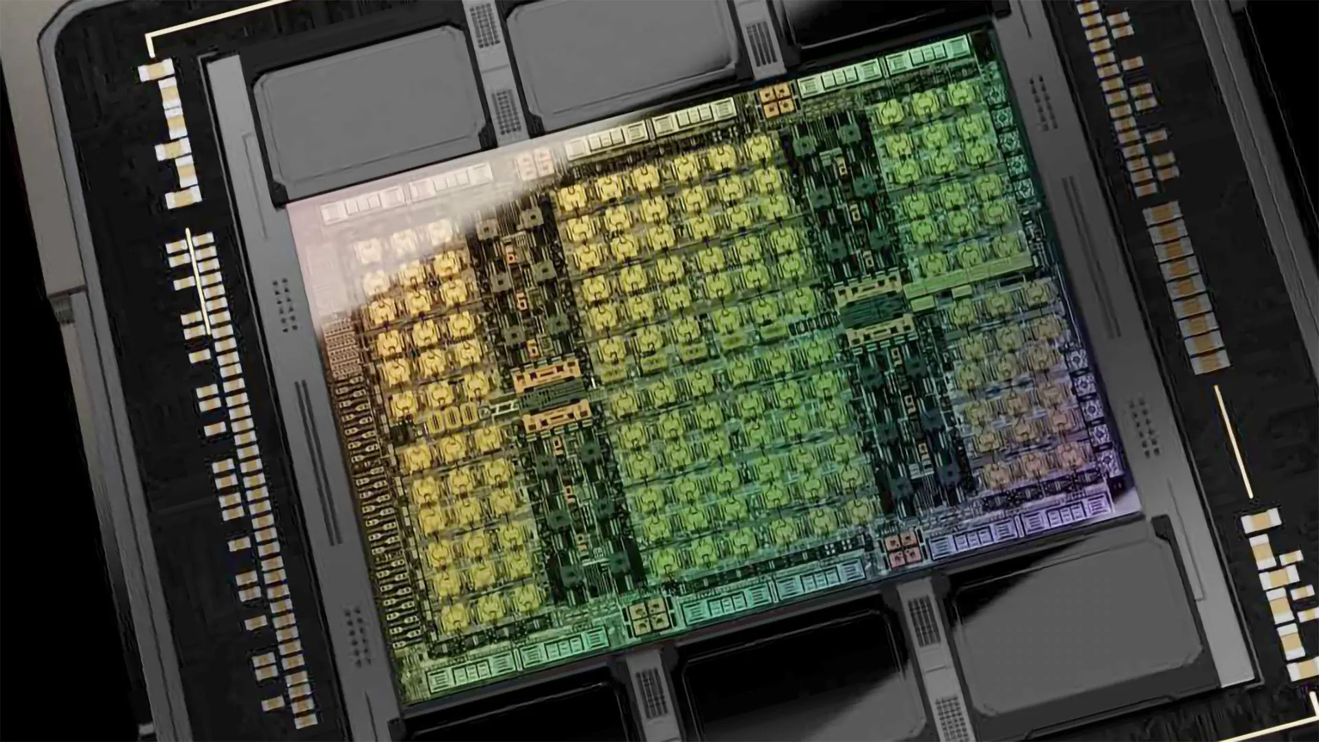
Nvidia's GA100 and GH100 compute GPUs feature a die size 826 mm² and 814 mm², which is very close to the maximum reticle size of 858 mm2. Producing such large chips with good yields is hard, but it looks like TSMC does it pretty well since Nvidia literally ships tons of H100 and A100 compute GPUs every quarter.
While Nvidia has consistently managed to increase performance of its compute GPUs quite tangibly with every new generation so far, reticle size is still an issue. Using a multi-chiplet design would enable Nvidia to add more transistors into its next-generation compute GPU and increase performance gain over its H100 more significantly than it would do with architectural improvements alone.
Since both AMD and Intel have already adopted multi-chiplet designs for their compute GPUs and will only further increase chiplet and transistor count going forward, Nvidia might not have a choice but to embrace a multi-tile design too. It remains to be seen whether the company would go with a dual-chiplet (like AMD's Instinct MI250) or multi-chiplet (like AMD's Instinct MI300 or Intel's Ponte Vecchio) approach, but the company just cannot ignore advantages presented by modern packaging technologies.
If we continue to speculate, we might assume that Nvidia will adopt multi-tile design only for its Blackwell GPUs for AI and HPC compute, whereas its gaming GPUs will remain monolithic. This might make sense since making two GPUs work in parallel is hard. But then again, Nvidia might not be able to ignore multi-chiplet designs even for client PCs in the High-NA era since ASML's next-generation scanners will halve reticle size (to 429 mm2) and Nvidia will not be able to address high-end gaming machines with monstrous monolithic GPUs like the AD102 (609 mm2) unless they use at least two chiplets.